- 您现在的位置:买卖IC网 > Sheet目录17351 > MC34063SMDBGEVB (ON Semiconductor)BOARD EVALUATION MC34063
�� �
�
�MC34063A,� MC33063A,� SC34063A,� SC33063A,� NCV33063A�
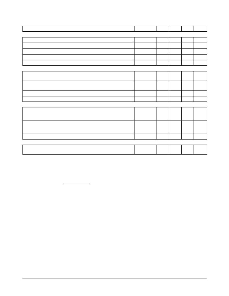
�ELECTRICAL� CHARACTERISTICS� (V� CC� =� 5.0� V,� T� A� =� T� low� to� T� high� [Note� 4],� unless otherwise� specified.)�
�Characteristics�
�Symbol�
�Min�
�Typ�
�Max�
�Unit�
�OSCILLATOR�
�Frequency� (V� Pin� 5� =� 0� V,� C� T� =� 1.0� nF,� T� A� =� 25� °� C)�
�Charge� Current� (V� CC� =� 5.0� V� to� 40� V,� T� A� =� 25� °� C)�
�Discharge� Current� (V� CC� =� 5.0� V� to� 40� V,� T� A� =� 25� °� C)�
�Discharge� to� Charge� Current� Ratio� (Pin� 7� to� V� CC� ,� T� A� =� 25� °� C)�
�Current� Limit� Sense� Voltage� (I� chg� =� I� dischg� ,� T� A� =� 25� °� C)�
�f� osc�
�I� chg�
�I� dischg�
�I� dischg� /I� chg�
�V� ipk(sense)�
�24�
�24�
�140�
�5.2�
�250�
�33�
�35�
�220�
�6.5�
�300�
�42�
�42�
�260�
�7.5�
�350�
�kHz�
�m� A�
�m� A�
�?�
�mV�
�OUTPUT� SWITCH� (Note� 5)�
�Saturation� Voltage,� Darlington� Connection�
�(� I� SW� =� 1.0� A,� Pins� 1,� 8� connected)�
�Saturation� Voltage� (Note� 6)�
�(I� SW� =� 1.0� A,� R� Pin� 8� =� 82� W� to� V� CC� ,� Forced� b� ]� 20)�
�DC� Current� Gain� (I� SW� =� 1.0� A,� V� CE� =� 5.0� V,� T� A� =� 25� °� C)�
�Collector� Off� ?� State� Current� (V� CE� =� 40� V)�
�V� CE(sat)�
�V� CE(sat)�
�h� FE�
�I� C(off)�
�?�
�?�
�50�
�?�
�1.0�
�0.45�
�75�
�0.01�
�1.3�
�0.7�
�?�
�100�
�V�
�V�
�?�
�m� A�
�COMPARATOR�
�Threshold� Voltage�
�T� A� =� 25� °� C�
�T� A� =� T� low� to� T� high�
�Threshold� Voltage� Line� Regulation� (V� CC� =� 3.0� V� to� 40� V)�
�MC33063,� MC34063�
�MC33063V,� NCV33063�
�Input� Bias� Current� (V� in� =� 0� V)�
�V� th�
�Reg� line�
�I� IB�
�1.225�
�1.21�
�?�
�?�
�?�
�1.25�
�?�
�1.4�
�1.4�
�?� 20�
�1.275�
�1.29�
�5.0�
�6.0�
�?� 400�
�V�
�mV�
�nA�
�TOTAL� DEVICE�
�Supply� Current� (V� CC� =� 5.0� V� to� 40� V,� C� T� =� 1.0� nF,� Pin� 7� =� V� CC� ,�
�V� Pin� 5� >� V� th� ,� Pin� 2� =� GND,� remaining� pins� open)�
�I� CC�
�?�
�?�
�4.0�
�mA�
�IC� driver� –� 7.0� mA� *�
�4.� T� low� =� 0� °� C� for� MC34063,� SC34063;� ?� 40� °� C� for� MC33063,� SC33063,� MC33063V,� NCV33063�
�T� high� =� +70� °� C� for� MC34063,� SC34063;� +� 85� °� C� for� MC33063,� SC33063;� +125� °� C� for� MC33063V,� NCV33063�
�5.� Low� duty� cycle� pulse� techniques� are� used� during� test� to� maintain� junction� temperature� as� close� to� ambient� temperature� as� possible.�
�6.� If� the� output� switch� is� driven� into� hard� saturation� (non� ?� Darlington� configuration)� at� low� switch� currents� (� ≤� 300� mA)� and� high� driver� currents�
�(� ≥� 30� mA),� it� may� take� up� to� 2.0� m� s� for� it� to� come� out� of� saturation.� This� condition� will� shorten� the� off� time� at� frequencies� ≥� 30� kHz,� and� is�
�magnified� at� high� temperatures.� This� condition� does� not� occur� with� a� Darlington� configuration,� since� the� output� switch� cannot� saturate.� If� a�
�non� ?� Darlington� configuration� is� used,� the� following� output� drive� condition� is� recommended:�
�IC� output�
�Forced� b� of� output� switch� :� w� 10�
�*� The� 100� W� resistor� in� the� emitter� of� the� driver� device� requires� about� 7.0� mA� before� the� output� switch� conducts.�
�http://onsemi.com�
�3�
�发布紧急采购,3分钟左右您将得到回复。
相关PDF资料
HCM06DRYN
CONN EDGECARD 12POS DIP .156 SLD
SJA7501-1-1/2-50-BLACK
LOOP BLACK 1 1/2" X 50YD X 0.12"
EBM11DRYH
CONN EDGECARD 22POS DIP .156 SLD
EEV-HB1C100R
CAP ALUM 10UF 16V 20% SMD
TARQ155K020
CAP TANT 1.5UF 20V 10% AXIAL
RE-243.3S/H
CONV DC/DC 1W 24VIN 3.3VOUT
L-07C4N3SV6T
CER INDUCTOR 4.3NH 0402
A9CCG-1005F
FLEX CABLE - AFG10G/AF10/AFG10G
相关代理商/技术参数
MC34063SMDBKEVB
功能描述:电源管理IC开发工具 MC34063A EVAL BRD
RoHS:否 制造商:Maxim Integrated 产品:Evaluation Kits 类型:Battery Management 工具用于评估:MAX17710GB 输入电压: 输出电压:1.8 V
MC34063SMDINVEVB
功能描述:电源管理IC开发工具 MC34063A EVAL BRD
RoHS:否 制造商:Maxim Integrated 产品:Evaluation Kits 类型:Battery Management 工具用于评估:MAX17710GB 输入电压: 输出电压:1.8 V
MC34063U
制造商:Motorola Inc 功能描述: 制造商:Motorola Inc 功能描述:1.5 A SWITCHING REGULATOR, 100 kHz SWITCHING FREQ-MAX, CDIP8
MC34064
制造商:MICROSEMI 制造商全称:Microsemi Corporation 功能描述:UNDERVOLTAGE SENSING CIRCUIT
MC34064D-005
功能描述:监控电路 4.59V UnderVoltage RoHS:否 制造商:STMicroelectronics 监测电压数: 监测电压: 欠电压阈值: 过电压阈值: 输出类型:Active Low, Open Drain 人工复位:Resettable 监视器:No Watchdog 电池备用开关:No Backup 上电复位延迟(典型值):10 s 电源电压-最大:5.5 V 最大工作温度:+ 85 C 安装风格:SMD/SMT 封装 / 箱体:UDFN-6 封装:Reel
MC34064D-005G
功能描述:监控电路 4.59V UnderVoltage Sensing Circuit RoHS:否 制造商:STMicroelectronics 监测电压数: 监测电压: 欠电压阈值: 过电压阈值: 输出类型:Active Low, Open Drain 人工复位:Resettable 监视器:No Watchdog 电池备用开关:No Backup 上电复位延迟(典型值):10 s 电源电压-最大:5.5 V 最大工作温度:+ 85 C 安装风格:SMD/SMT 封装 / 箱体:UDFN-6 封装:Reel
MC34064D5
制造商:ON Semiconductor 功能描述:VOLT SENSE CCT SMD 34064 SOIC8
MC34064D-5
制造商:ON Semiconductor 功能描述: